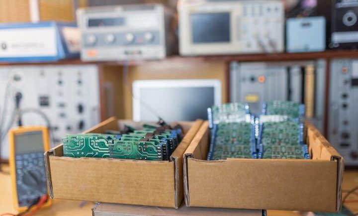
Semiconductor Packaging Materials: Types, Uses and Trends
Semiconductor packaging materials protect chips, connect electrical pathways, manage heat, and support reliable operation in modern electronic devices.
Semiconductor packaging materials are the materials used to protect an integrated circuit after fabrication and connect it with the wider electronic system. Packaging provides mechanical protection, electrical connections, thermal management, and environmental resistance.
Modern semiconductor packaging can involve several material categories, including:
- Encapsulation materials: Protect the semiconductor die from moisture, contamination, and mechanical damage.
- Substrates: Provide electrical pathways and mechanical support between the chip and circuit board.
- Leadframes: Support semiconductor dies and provide external electrical connections.
- Solder materials: Create electrical and mechanical connections between package components.
- Underfill materials: Improve reliability around connections such as flip-chip structures.
- Thermal interface materials: Help transfer heat away from high-power semiconductor devices.
- Glass and ceramic materials: Used where electrical insulation, dimensional stability, or specialized thermal characteristics are important.
Packaging has become increasingly sophisticated because smaller chips and higher processing performance can increase thermal, electrical, and mechanical challenges.
Why Packaging Materials Matter Today
Semiconductor packaging is no longer simply a protective outer layer. It is an important part of semiconductor engineering and can influence signal integrity, heat dissipation, reliability, and overall system performance.
Advanced semiconductor packaging includes approaches such as 2.5D packaging, 3D packaging, chiplet integration, fan-out packaging, system-in-package (SiP), and heterogeneous integration.
These approaches are particularly relevant to applications involving artificial intelligence, high-performance computing, telecommunications, automotive electronics, industrial systems, and data-center infrastructure.
Material selection therefore involves balancing properties such as thermal conductivity, electrical insulation, coefficient of thermal expansion, moisture resistance, mechanical strength, and long-term reliability.
High-value technical areas include: semiconductor packaging technology, advanced packaging materials, chiplet packaging, semiconductor substrate materials, thermal management materials, electronic materials engineering, and IC packaging technology.
Recent Industry Developments
The semiconductor packaging landscape has continued to develop during 2025 and 2026, particularly around advanced packaging and domestic manufacturing capacity.
India Semiconductor Mission information published in 2025 highlighted advanced packaging, heterogeneous integration, and related technologies as important areas for India's semiconductor ecosystem.
India's semiconductor program also recorded several packaging-related project developments during 2025. These included approved projects involving OSAT facilities and advanced packaging technologies. A 2025–26 Ministry of Electronics and Information Technology report also described projects involving glass substrates, 3D heterogeneous integration, SiC semiconductor packaging, and OSAT capacity.
| Packaging area | Typical material focus | Main purpose |
|---|---|---|
| Flip-chip | Solder, underfill, substrate | Electrical interconnection |
| Fan-out | Mold compounds, redistribution materials | Compact integration |
| 2.5D/3D | Interposers, substrates, bonding materials | High-density integration |
| Power packaging | Thermal materials, ceramics | Heat management |
| SiP | Multiple semiconductor and passive materials | System integration |
These developments are increasing attention on material characterization, thermal management, reliability testing, and advanced substrate technologies.
Laws, Policies and Standards
In India, semiconductor packaging is connected with the country's broader electronics and semiconductor manufacturing framework.
The India Semiconductor Mission identifies semiconductor ATMP and OSAT facilities as part of its semiconductor ecosystem. Its published scheme information describes fiscal support for eligible semiconductor packaging facilities.
Environmental requirements can also affect material selection. India's E-Waste Management Rules, 2022 contain provisions concerning restricted substances and specific exemptions involving materials used in electronic equipment, including certain semiconductor-related solders.
Manufacturers and engineers may also need to consider applicable product standards, environmental requirements, chemical restrictions, workplace controls, and international customer specifications when selecting packaging materials.
Tools and Resources for Learning
Useful resources for understanding semiconductor packaging include:
- Material property databases for thermal, electrical, and mechanical characteristics
- Thermal simulation tools for evaluating heat transfer and package temperatures
- Finite-element analysis tools for mechanical and thermal modeling
- Reliability calculators for estimating thermal cycling and material stresses
- Package design templates for documenting layer structures and material specifications
- Semiconductor standards databases for researching testing and qualification requirements
- Government semiconductor portals for policy and program information
These resources can help readers understand why different materials are selected for different package architectures.
Frequently Asked Questions
What are semiconductor packaging materials?
They are materials used to protect semiconductor dies, create electrical connections, provide mechanical support, and manage heat within an electronic package.
Which materials are commonly used in chip packaging?
Common categories include polymers, epoxy-based compounds, silicon, metals, ceramics, glass, solder materials, substrates, and thermal interface materials.
Why is thermal management important in semiconductor packaging?
Higher-power chips can generate substantial heat. Effective thermal pathways help maintain operating temperatures and support long-term reliability.
What is advanced semiconductor packaging?
It refers to packaging approaches that integrate chips, chiplets, interconnects, and other components in increasingly compact and high-performance configurations.
Is semiconductor packaging important for AI hardware?
Yes. AI processors can require high bandwidth, dense interconnections, and substantial thermal management, making advanced packaging technologies particularly relevant.
Conclusion
Semiconductor packaging materials play a fundamental role in modern electronics. They provide protection, electrical connectivity, mechanical stability, and thermal management while supporting increasingly complex chip architectures.
The growing adoption of advanced packaging, chiplets, heterogeneous integration, and high-performance computing is also increasing the importance of material engineering. In India, government semiconductor initiatives and new packaging projects are contributing to the development of a broader domestic ecosystem.
Disclaimer: This article is for general educational purposes. Material selection, semiconductor qualification, environmental compliance, and packaging design should be evaluated using applicable technical standards, regulations, and engineering specifications.